Description
Brisk-AFM UK
Atomic Force Microscopy ( AFM) also known as Scanning Force Microscopy (SFM) is very high resolution type of Scanning Probe Microscopy (SPM) with a benefit of 1000 times better than Optical Diffraction limit. Resolution in the order of a nanometer
Scanning Probe Microscope, (AFM-SFM) from our group company Brisk-afm UK
Optical Microscope’s inability to image sizes smaller than a wavelength of visible light resulted in the invention of nano-scopes in the last decade.
AFM is at the top of the list, due to its low price and multi-applications.
The basic principle of AFM
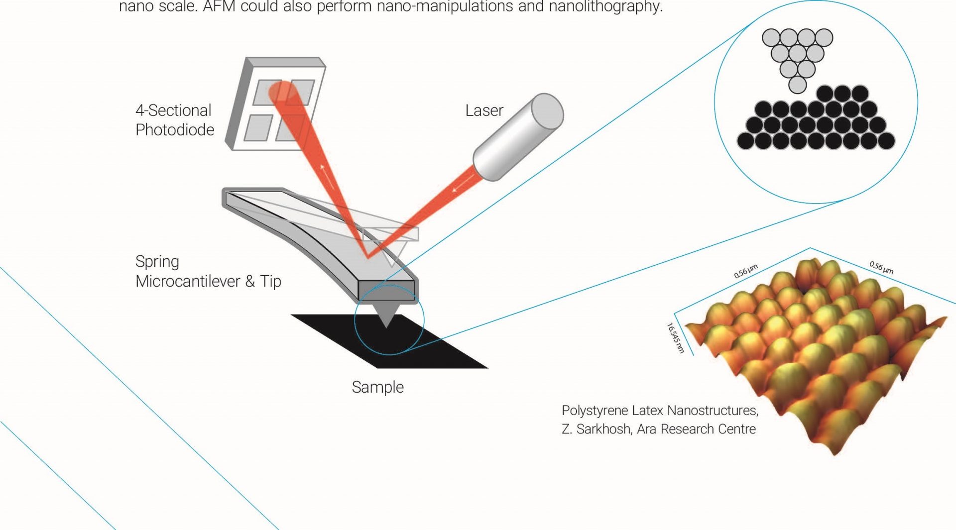
A spring micron size cantilever has a conical tip at its free end. The conical tip with a very sharp end, usually less than 10 nanometres, scans the sample surface from a very close nanometric distance.
As the tip moves over the surface the Van Der Waals forces between atoms on the sharp end of the tip, as a side note the tip is one atom in diameter, and the atoms on the surface of the sample varies, resulting vertical displacements of the cantilever.

Vertical movements of the cantilever are reflected using a laser to magnify the movement of the cantilever.
The reflected laser beam from the cantilever’s highly polished upper surface hits a quadruple photodiode.
The output signals of the photodiodes are related to the vertical movements of the cantilever which in turn represents the surface topography of the sample.
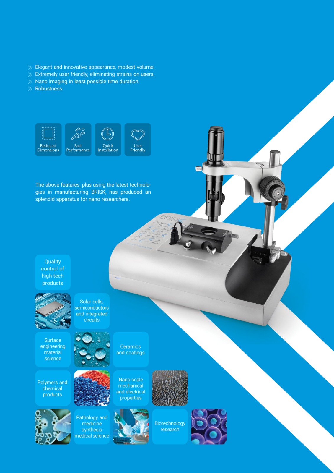
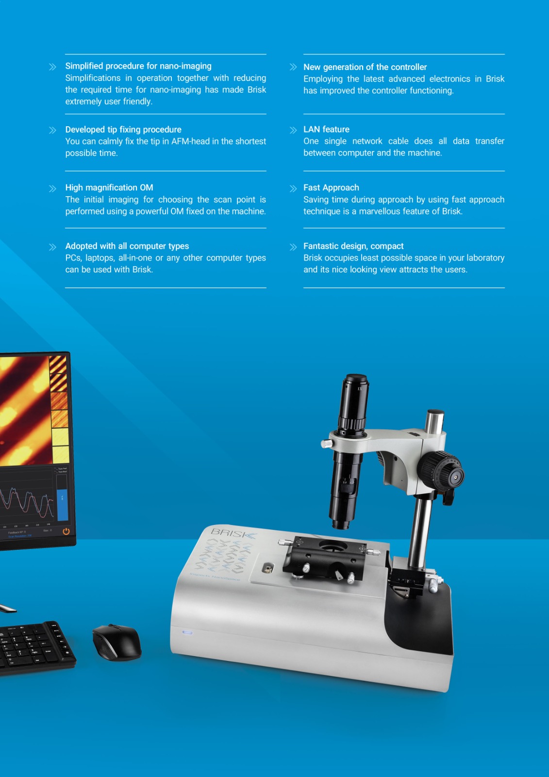
The whole system is light weight, portable and accurate.
Easy to use.
Functional Modes
Standard Version Modes:
- Contact, Non-Contact, Tapping, Phase image, Lateral Force Microscopy (LFM)
Advanced Version Modes:
- Magnetic Force Microscopy (MFM), Electric Force Microscopy (EFM), Force Spectroscopy + All Standard Modes
Full Version Modes:
- Chemical and Mechanical Nano-Lithography, Force Modulation Microscopy (FMM) + All Advanced Modes
Full Plus Version Modes:
- Kelvin Probe Force Microscopy (KPFM), Conductive AFM (C-AFM), Piezo-response Force Microscopy (PFM), Frequency Modulation (FM) + All Full Modes
Applications
- Biological
- Non Biological
- Atomic: Scale imaging solid surface
- Atom and Nano Structure manipulation
- Spectroscopy of sample at desired area
- Opto-electronics
- Surface materials
- semiconductor
- Chemistry
- Solid-state physics
- Medicine
- plus many more to mention
Scanner
- XY Scanner
- 50 pm Maximum XY scan range
- 1 nm XY resolution
- Z Scanner
- 4 pm Maximum Z scan range
- 0.1 nm Z resolution
Stage
- XY Stage
- Software-controlled motorized stage for sample positioning
- 15 mm Stage travel range
- 40 nm XY Stage steps
- Z Stage
- 15 mm Stage Z travel range
- 40 nm Z Stage steps
- Automatic engage of the cantilever to the sample surface (Auto Fast Approach)
Sample Mount
- 20 mm Maximum sample diameter
- 10 mm Maximum sample thickness
- Includes light magnetic sample holder
- 10 V to +10 V Bias voltage range to the sample
Top View Optical Microscope
- 8-MegapixeI resolution,
- Colour to Optical zoom
- Integrated lighting
- Include microscope dimmer
5 mW Maximum laser diode power
- Electronics
- ADC and DAC Channels
- 4 Channel ADC 24bit
- 4 Channel DAC 24bit
- Signal processing
- 40 MHz frequency zinc processor
- Integrated functions
- 100 MB/sec via LAN

